FG Interface schematics and PCBs: Difference between revisions
Jump to navigation
Jump to search
m (WIP) |
m (adding low level schemas) |
||
| Line 2: | Line 2: | ||
You will find in this section, all the plans, diagrams, PCB ... etc, in short all that relates to hardware for FG Interface and its construction. | You will find in this section, all the plans, diagrams, PCB ... etc, in short all that relates to hardware for FG Interface and its construction. | ||
Examples of panels can be presented and documented. | Examples of panels can be presented and documented. | ||
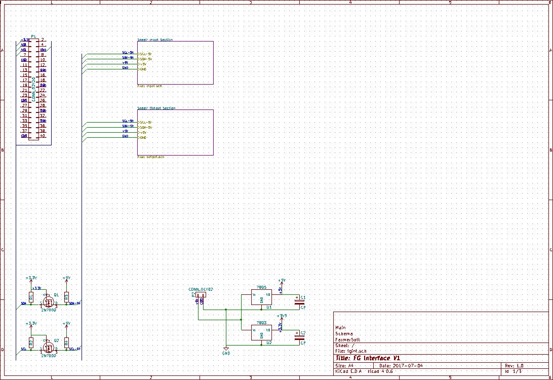
[[File:FG_Interface_1_Main_Layer.jpg]] | |||
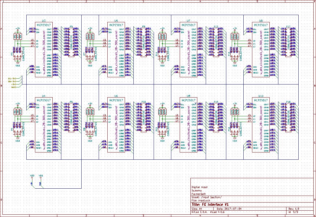
[[File:FG_Interface_1_Digital_Inputs.jpg]] | |||
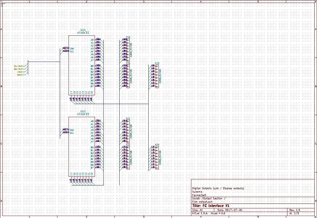
[[File:FG_Interface_1_Digital_Output.jpg]] | |||
{{WIP}} | {{WIP}} | ||
Revision as of 22:36, 11 July 2017
| FG Interface hardware |
|---|
|
Raspberry PI Setup
|
|
Navigation |
You will find in this section, all the plans, diagrams, PCB ... etc, in short all that relates to hardware for FG Interface and its construction.
Examples of panels can be presented and documented.


| Work in progress This article or section will be worked on in the upcoming hours or days. See history for the latest developments. |